FPGA-Based Text Editor

This project is a terminal‑based text editor designed for the Cyclone V GX FPGA. It transforms the FPGA into a standalone text‑editing device: you can create text, modify it, store it in Block RAM, view the output on a HDMI monitor, and finally transmit the completed text to a PC via UART.
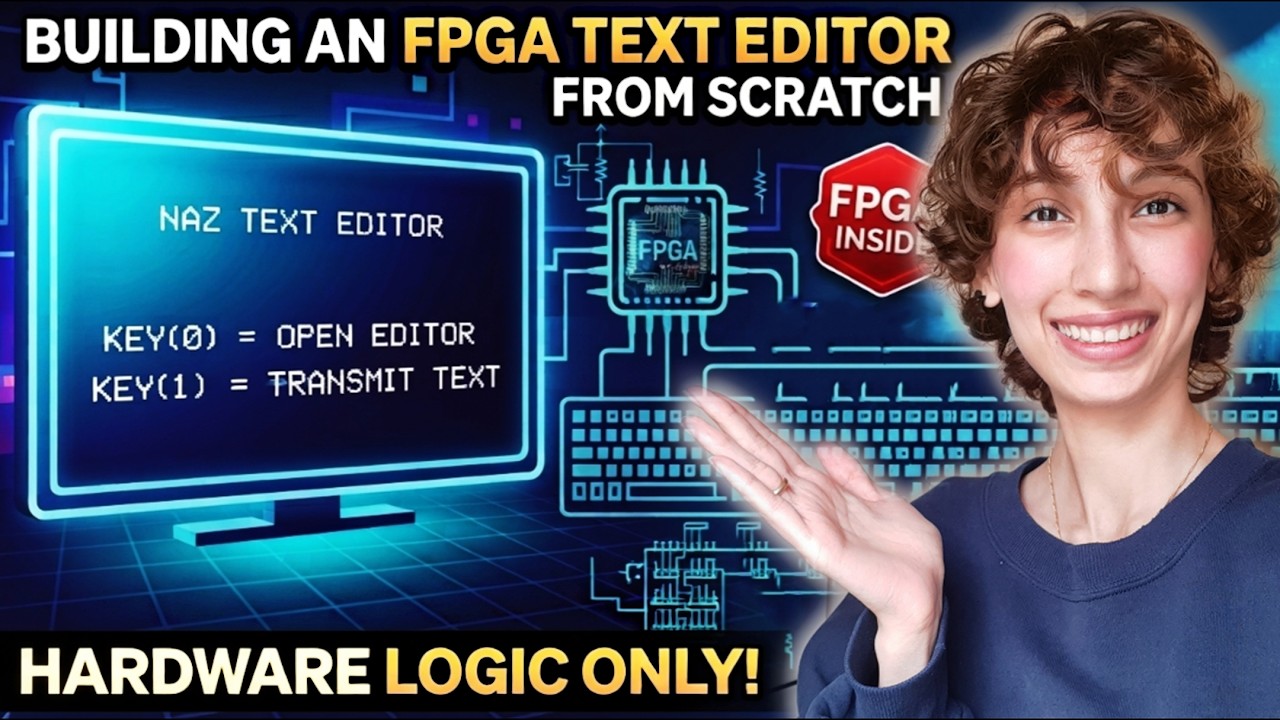
Watch the demo on youtube (click on the picture below):
Project Overview
This system turns the FPGA into a fully functional text editor. By connecting a serial terminal and a HDMI display, you can type characters that are stored in the FPGA’s internal memory and rendered on‑screen in real time. The editor supports a 640×480 resolution and provides space for 4,800 characters (80 columns × 60 rows). When you finish editing, the entire text buffer can be sent to a PC over UART, where a Python script saves it as a standard text file.
Data Flow
In this section, I explain exactly how this Text Editor works, so feel free to read this part to understand the data flow.
Data Input (Keyboard to FPGA)
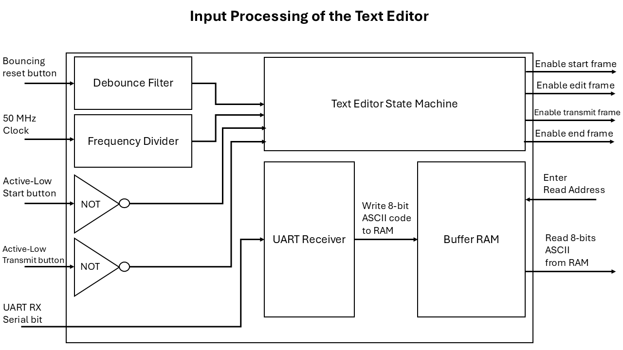
The process begins when I press a key on my computer keyboard. My PC then sends the ASCII code for that key as a serial signal through its UART transmitter to the FPGA. The UART transmitter of the PC sends one start bit, 8‑bit ASCII data, and one stop bit.
The UART_RX module on the FPGA receives this ASCII code bit‑by‑bit. The UART_RX module is configured to handle 8 bits of data with one start bit and one stop bit (which exactly matches the way the PC transmitter sends the data). Once the module receives all bits, it converts them into a parallel 8‑bit format (ASCII code).
Storage in the Character Buffer
After the FPGA receives the ASCII code, it must store it so it can be displayed and eventually saved.
The char_buffer module acts as the system’s memory. This module contains a RAM organized into a grid of 80 columns and 60 rows, meaning it has a total of 4800 locations. Each location of this RAM can hold 1 byte of ASCII code, so in total 4800 bytes of data can be stored.
When the FPGA receives the ASCII data of each character, it stores it in the RAM. The character is placed into a specific memory address that corresponds to the current typing position on the screen.
Display the Text on Monitor
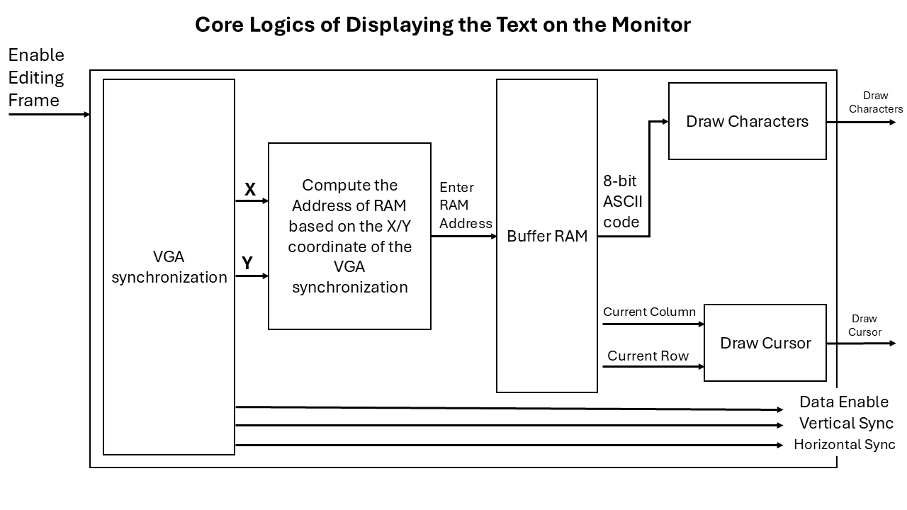
While I am typing, the system constantly updates the monitor so I can see my text. The VGAsync module generates the timing signals (Horizontal and Vertical Sync) needed for a 640×480 resolution at 60 Hz. As the X/Y coordinates of the VGAsync module move across the screen, the draw_characters module fetches the ASCII codes from the RAM buffer. It uses the font_pack package to translate these codes into 8×8 pixel images (the image of each letter, digit, or symbol). Simultaneously, the draw_cursor module creates a blinking box on the screen to show exactly where the next character will be placed.
Data Export (FPGA to PC)
When I finish editing, I can send my text back to the PC to save it as a permanent file.
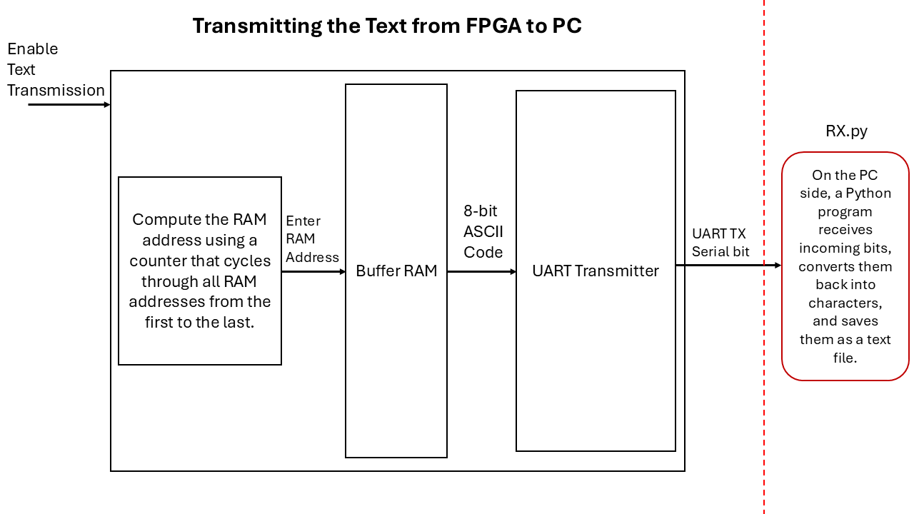
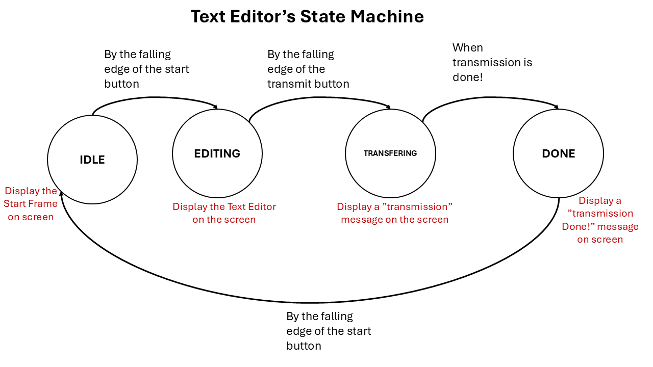
When I press the transmission button on the board, the txt_editor_FSM switches to the TRANSFERRING state.
The UART_TX module reads the ASCII characters from the buffer one by one and sends them back to the PC bit‑by‑bit at a baud rate of 115200.
On the PC side, the RX.py script is running. It listens to the serial port, collects the incoming bits, and converts them back into characters. Finally, it saves the complete text into a file named fpga_text_output.txt.
The Text Editor’s State Machine
The overall behavior of the system is managed by the txt_editor_FSM. The system remains in the IDLE state until it is triggered to enter EDITING mode. When the text is finished and a physical transmission button is pressed, the state changes to TRANSFERRING to begin the export process. when the transmission is done, the systems moves into DONE state.
The Logic Behind The System
There are three important logics behind this text editor.
The Screen Grid Logic
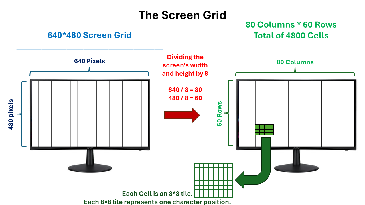
The screen grid is the logic that divides the screen into small squares for text. The monitor has a resolution of 640x480 pixels. Instead of treating it as one big image, the system divides it into small tiles of 8x8 pixels each.
If we divide 640 by 8, we get 80 columns, and if we divide 480 by 8, we get 60 rows. This grid creates a total of 4,800 available slots (80 × 60) for characters to be placed on the screen.
The Block RAM Logic
As I said in the data flow section, the char_buffer is the internal memory where our typing is actually saved. The reason that I have chosen this buffer to have exactly 4800 locations is to match the number of slots in the screen grid.
So each screen slot is connected to its corresponding location in RAM; whatever ASCII value is stored in that location of RAM will be displayed on the screen.
The Font Pack Logic
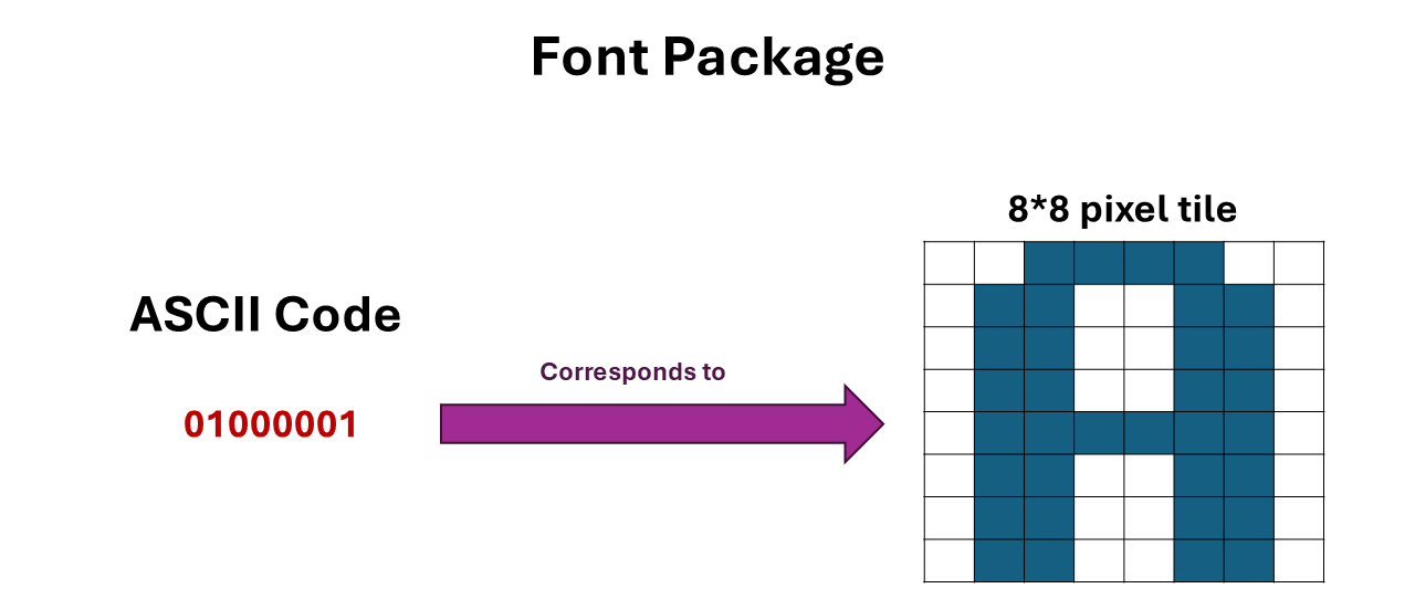
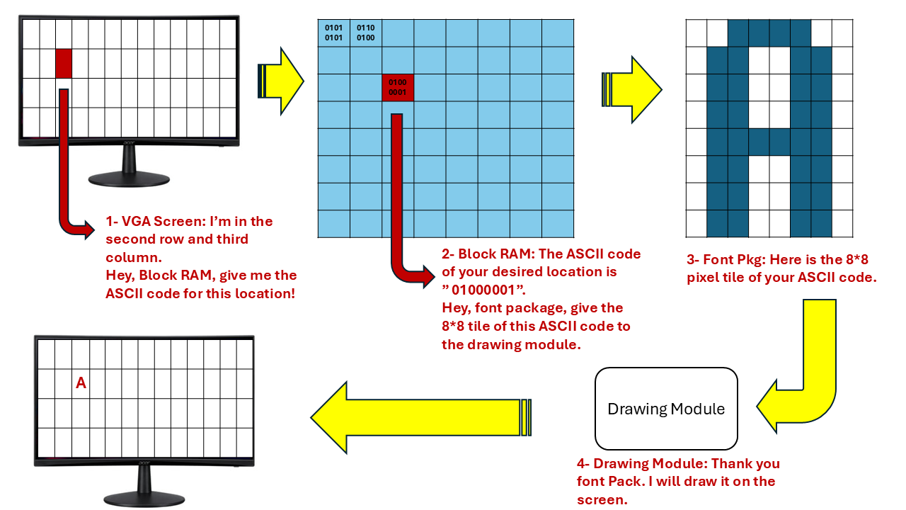
The font_pack is the library that explains how to draw each character. The font pack defines every character as an 8x8 grid of bits. For example, for the letter “A,” the font pack tells the system which specific pixels in that 8x8 box should be turned on (colored) and which should be off (background).
When the system wants to draw a character, it looks at the ASCII code in the block RAM and then asks the font_pack for the corresponding 8x8 pixel pattern.
How They Work Together Simply:
The Screen Grid identifies a location on the monitor (for example, Column 10, Row 5).
The Character Buffer looks at that specific address in its memory to see which ASCII code is stored there.
The Font Pack provides the 8x8 pixel pattern for that ASCII code so the draw_characters module can light up the correct pixels on screen.
Setup Guide
The project has been tested on Altera Cyclone V GX Starter Kit. For this Board, I have used the follwing Pinout table:
Click here to open the Pinout-Table.CSV
Compilation Report
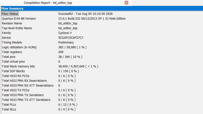
Here is the compilation report for the text editor.
The resources used to implement this terminal‑based text editor on the Cyclone V GX FPGA include 382 ALMs, 209 registers, 38 pins, and 38,400 block RAM bits.